

When the Original Design is Lost: TECOO’s Complete Guide to PCB Reverse Engineering & File Recovery
Nov 19, 2025
Have you ever faced this common challenge in electronics development?
A successful product generating steady revenue may lose its original design files-schematics, PCB layouts-due to personnel changes or poor archiving.
An industrial control system may require an upgrade or repair, but the original manufacturer is gone and no technical documentation exists.
You may want to analyze a competitor's product to understand its design or ensure interoperability with your own devices.
In these cases, PCB reverse engineering becomes the solution to reviving and improving products. With decades of expertise in PCB file extraction, circuit analysis, and PCBA cloning, TECOO can restore and optimize your designs safely and efficiently.
What is PCB Reverse Engineering?
PCB reverse engineering (also called PCB cloning) involves analyzing physical PCBs with advanced techniques to recover original design data-schematics, layout files, and bills of materials (BOM).
Legal Compliance: TECOO strictly operates within all laws and intellectual property regulations. Services are limited to legal use cases such as:
- Recovering proprietary design data
- Academic research or teaching
- Interoperability or compatibility analysis
- Repair and iteration of discontinued devices
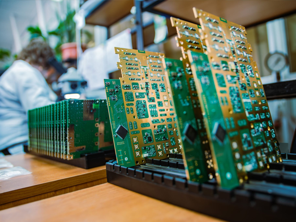
Core PCB Reverse Engineering Process: From Physical Board to Production Files
PCB reverse engineering is a systematic process that requires deep circuit knowledge, specialized tools, and attention to detail. The workflow typically includes:
Step 1: Preparation and Non-Destructive Analysis
- High-Definition Imaging: Photograph or scan both PCB sides to capture the original state.
- Component Identification & BOM Generation: Record every component, its package, and tag number (e.g., R1, C2, U3).
- Software/Firmware Extraction: For pre-programmed chips (MCUs, CPLDs, Flash), TECOO uses professional tools to safely extract firmware when necessary.
Step 2: Layer-by-Layer Peeling and Trace Mapping
- Component Removal & Board Cleaning: Carefully remove components and clean the board for trace visibility.
- Scanning & Image Processing: Use high-definition scans and software adjustments for clear trace mapping.
- Trace & Via Reconstruction: Engineers trace each copper line and via, restoring the full physical layout, including stack-up structures for multi-layer boards.
Step 3: Schematic Reconstruction
- Drawing the Schematic: Translate the PCB layout into human-readable schematics using EDA software (Altium Designer, KiCad).
- Circuit Analysis & Module Division: Identify functional blocks-power modules, MCU systems, analog processing, communication interfaces (USB, UART)-for clarity and logical accuracy.
- Cross-Verification: Compare schematics with the physical board and BOM to ensure accuracy and correct errors.
Step 4: File Generation & Production Readiness
Output Production Files:
- Gerber files for PCB fabrication
- Drill files for PCB drilling
- Coordinate files for SMT machines
- BOM for component sourcing
DFM Analysis:
Check manufacturability to prevent mass production issues.
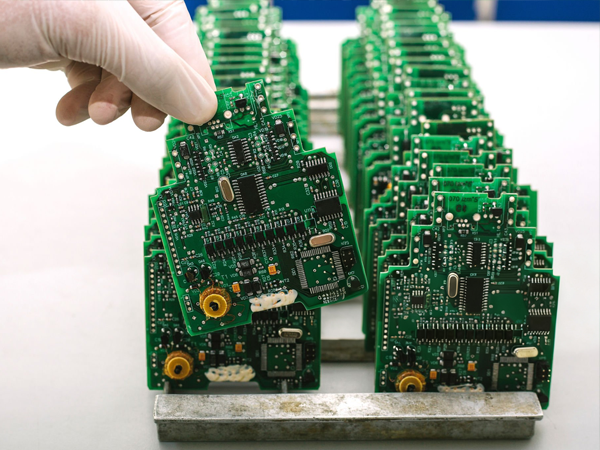
Why TECOO Stands Out in PCB Reverse Engineering
- Expert Engineering Team: We understand "why" a design works, not just "how it looks," allowing error detection and optimization.
- Advanced Tools & Technology: From high-definition scanning to firmware extraction, we use cutting-edge equipment to ensure efficiency and accuracy.
- End-to-End Service: From file extraction and BOM optimization to PCBA cloning, we provide a one-stop solution.
- Meticulous Quality Control: Every trace, via, and component is verified to match the original board's functionality.
Conclusion: Recover, Optimize, and Upgrade
Lost design files don't have to mark the end of your product lifecycle. TECOO's professional PCB reverse engineering helps you:
- Recover lost schematics and layouts
- Analyze and optimize original designs
- Upgrade performance, reduce costs, and strengthen your supply chain
Contact TECOO today to recover your lost "blueprint" and bring your products back to life.
You Might Also Like
-
High-Precision Medical PCBA Solutions For Healthcare Devices
-
14pcs Servos Robotic Arm Driver Control Board
-
OEM PCB Manufacture Assembly PCBA Circuit Board For Weldi...
-
Cost-Effective Robot Arm Control Brushless DC Motor Drive...
-
PCBA OEM Service New Energy Charging Pile PCB Board Print...
-
High-Precision Automatic Door Controller PCB Assembly